TM 11-6125-240-34
NOTES:
1.
UNLESS
OTHERWISE
INDICATED,
3.
INDICATES
RESISTANCES ARE IN OHMS,
EQUIPMENT MARKINGS
CAPACITORS ARE IN UUF,
4 RECEPTACLE VIEWED
2. UNLESS OTHERWISE INDICATED,
FROM PIN OR RECEPTACLE
ALL WATTAGE RATINGS OF
SIDE
RESISTORS ARE 1/2 WATT.
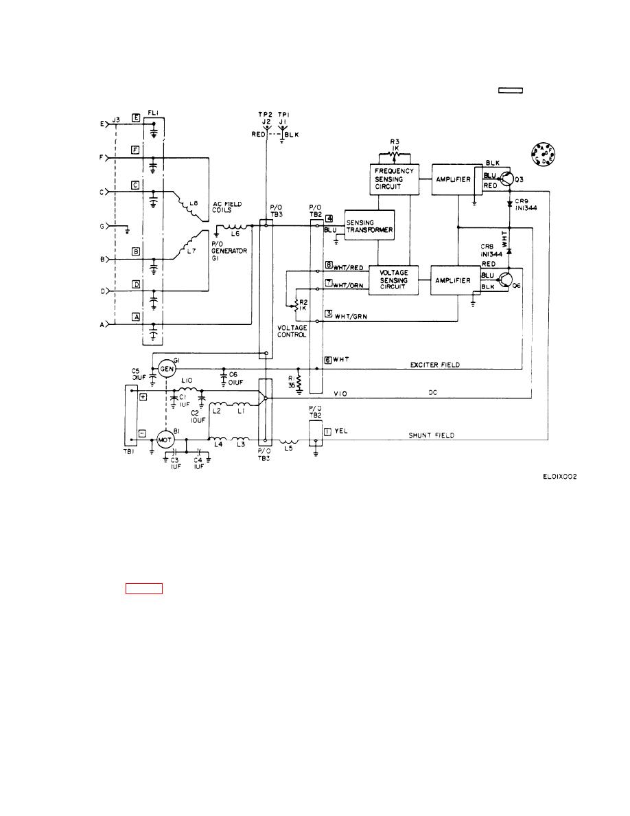
Figure 2-2. Motor-Generator PU-545/A with CSV1186-1 Regulator, Simplified Schematic Diagram
Section IV. CIRCUIT ANALYSIS, CSV2215-2 AND CSV2215-3
Q5, which determines the length of on- or off-time of
2 - 7 . Voltage Regulation (CSV2215-2 and
the power transistor Q7. Any increase in differential
CSV2215-3)
voltage will cause a decrease in on-time of power tran-
sistor Q7, resulting in a lower field current in the
generator, and a corresponding drop in output voltage.
nected to positive dc and the other side is connected to
Any decrease in differential voltage will increase the
the collector of power transistor Q7. When power tran-
on-time of Q7, with a corresponding increase in output
sister Q7 is on, total dc voltage appears across the field.
voltage.
When transistor Q7 is off, total dc voltage appears
c. The regulator reacts instantaneously to any
across the transistor.
change in output voltage and maintains it constantly
b. The sensing voltage is taken from the output ter-
at a preset value. Free-wheeling or commutating diode
minal of the generator and applied to the sensing cir-
CR8 is used to provide a path for the field current dur-
cuit, where it is compared with the voltage in the
ing the off-time of power transistor Q8.
breakdown Zener diode (CR7) circuit. The differential
of these voltages is fed to the base of driver transistor
2-5


